
PhD scholars in hardware and silicon design, your breakthrough moment arrives! Google offers the Silicon Engineering Internship for Summer 2026 in Bengaluru, targeting advanced researchers to work on cutting-edge TPUs and cloud silicon. Fully funded with stipend, this 12-14 week program shapes Google’s hardware future. Apply now via careers.com – competition is fierce for Bengaluru spots!
Google’s Bengaluru campus leads Cloud hardware innovation alongside Hyderabad. Perfect for ECE/EE PhD candidates passionate about silicon engineering internships India. Detailed breakdown, eligibility, and application steps ahead!
Read More: Free Data Science Internship by Microsoft Karnataka [Travel – Less than 25%] Apply!
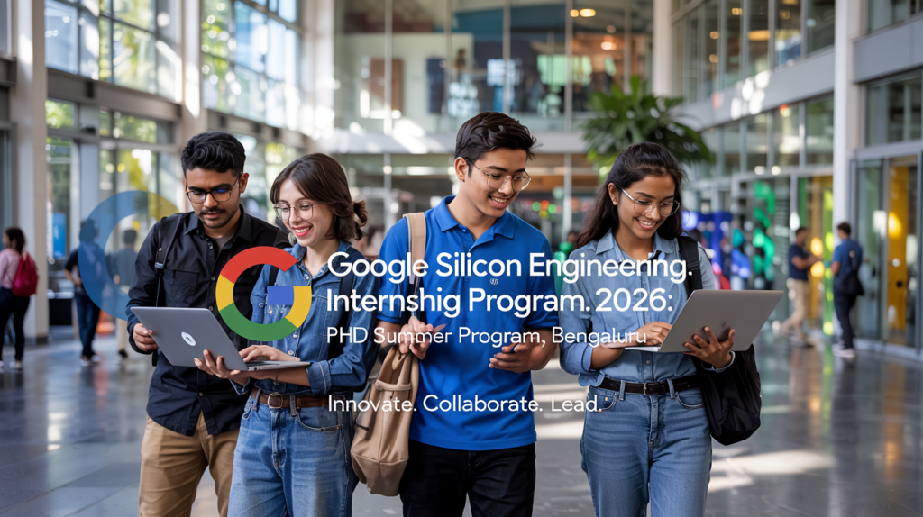
Table of Contents
Read More: Free Remote Data Science Internship at MNJ SOFTWARE – Apply Now | Salary ₹2-4 LPA | Apply!
Program Overview: Silicon Engineering Internship
The Silicon Engineering Intern, PhD, Summer 2026 immerses you in Google’s Cloud Silicon team, developing Tensor Processing Units (TPUs), Arm servers, and network ASICs. Expect hands-on chip design, verification, and deployment for global cloud infrastructure.
Key details:
- Duration: 12-14 weeks (May-August 2026, exact dates TBD).
- Location: Bengaluru, Karnataka, India (primary; Hyderabad alternate).
- Eligibility: PhD students graduating 2026-2028.
- Compensation: Competitive stipend + housing/relocation support.
- Team Focus: Hardware engineering for Google Cloud scalability.
This elite program outshines university research, offering production silicon impact.
About the job
As a Hardware Engineering Intern, you will work in a team that is shaping the future of Google Cloud Silicon, including TPUs, Arm based servers and network products. You will collaborate with hardware and software architects and designers to architect, model, analyze, define and design next-generation Cloud Silicon. You will have dynamic, multi-faceted responsibilities in areas such as product definition, design and implementation, collaborating with the Engineering teams to drive the optimal balance between performance, power, features, schedule and cost.
The ML, Systems and Cloud AI (MSCA) organization at Google designs, implements and manages the hardware, software, machine learning and systems infrastructure for all Google services (e.g., Search, YouTube, etc.) and Google Cloud. Our end users are Googlers, Cloud customers and people who use Google services around the world.
We prioritize security, efficiency and reliability across everything we do – from developing our latest Cloud Si products to running a global network, while driving towards shaping the future of hyperscale computing.
About the Role
is and always will be an engineering company. We hire people with a broad set of technical skills who are ready to address some of technology’s greatest challenges and make an impact on millions, if not billions, of users. At Google, engineers not only revolutionize search, they routinely work on massive scalability and storage solutions, large-scale applications and entirely new platforms for developers around the world. From Ads to Chrome, Android to YouTube, Social to Local, engineers are changing the world one technological achievement after another.
Responsibilities: Shape Future TPUs
Interns drive real silicon projects at Bengaluru:
- RTL Design: Code Verilog/SystemVerilog for custom accelerators.
- Verification: Develop UVM testbenches, simulate with VCS/Incisive.
- Synthesis & Timing: Optimize for TSMC nodes using Synopsys tools.
- Power Analysis: Profile chip efficiency for cloud workloads.
- Team Collaboration: Weekly syncs with architects, firmware engineers.
- Documentation: Publish internal design specs, contribute to patents.
Work alongside PhDs who’ve shipped TPU v4/v5 – unparalleled for silicon design careers.
Who Qualifies? Strict PhD Requirements
Google targets top-tier researchers:
- Education: Enrolled PhD (EE/ECE/CS) from recognized Indian/global unis; 3+ years coursework.
- Technical Skills: RTL (Verilog/VHDL), digital design, scripting (Python/Perl).
- Tools Expertise: Cadence/Synopsys suite, simulation, emulation.
- Experience: Prior silicon internships/research; publications at ISCA/MICRO.
- GPA: 8.5+ CGPA equivalent; strong recommendation letters.
- Visa: Indian nationals preferred; work authorization required.
IIT/IISc students dominate, but NIT/BITS standouts compete well.
Why Silicon Internship? Transformative Perks
Beyond stipend, unlock lifelong advantages:
- World-Class Mentorship: Report to TPU architects, ex-Apple/Intel leads.
- Cutting-Edge Tech: Design next-gen 3nm silicon for AI workloads.
- Global Network: Collaborate with Mountain View, Malmo teams.
- Compensation: ₹1.5-2.5L/month stipend + flights, PG accommodation.
- PPO Path: 50%+ convert to Hardware Engineer roles at ₹50+ LPA.
- Prestige: “Google Silicon Intern” opens doors at NVIDIA, Qualcomm.
| Benefit | Silicon Intern | Typical PhD Internship |
|---|---|---|
| Projects | Production TPUs | Academic prototypes |
| Mentors | Principal Engineers | Professors |
| Tools Access | Latest Synopsys | University licenses |
| Stipend | ₹1.5-2.5L/month | ₹20-50k |
| PPO Rate | 50%+ | <10% |
| Duration | 12-14 weeks | 8 weeks |
Read More: Sales Operations Analyst Trainee- Non-Technical Graduate Apprentice- Bangalore Apply Now!
Application Process: 4-Round Selection
Apply immediately on careers portal:
- Submit Online: careers.google.com → “Silicon Engineering Intern PhD 2026” → Bengaluru.
- Resume Screening: 1-page CV + research statement (500 words).
- Online Assessment: RTL coding, digital logic (1.5 hours).
- Interviews: 4x45min rounds – RTL design, verification, system, behavioral.
- Offer: Virtual coffee chat; relocation packet.
- Timeline: Apps open Jan-Mar; decisions by April.
Prep Hack: Practice “Design a TPU systolic array” problems; study Google SRE book.
How to Apply?
If you are an Interested Candidate, you can apply for the Google Silicon Engineering Internship 2026: PhD Summer Program, Bengaluru – Stipend Included! Click Here.